
Microstructure analysis with SEM

Microstructure analysis with SEM
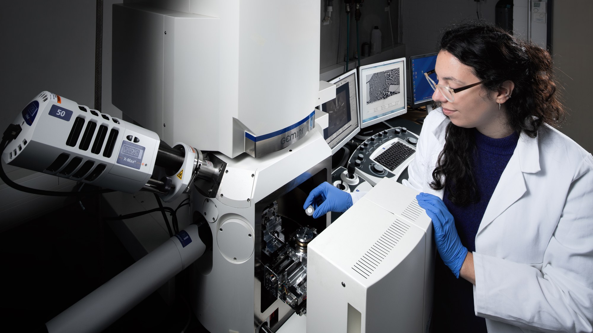
Scanning electron microscopy (SEM) enables the imaging of material surfaces using a focused electron beam. Microstructures and topography of materials can be analysed, and with the help of the energy dispersive X-ray spectroscopy (EDX) and electron backscatter diffraction (EBSD) detectors, both composition and crystalline structures can be determined at the nanometer scale.
Credit: © DLR. All rights reserved