August 19, 2025 | DLR achieves breakthrough in materials research
Peering into the atomic realm with matter waves
DLR researchers have succeeded in diffracting an atom beam through a solid
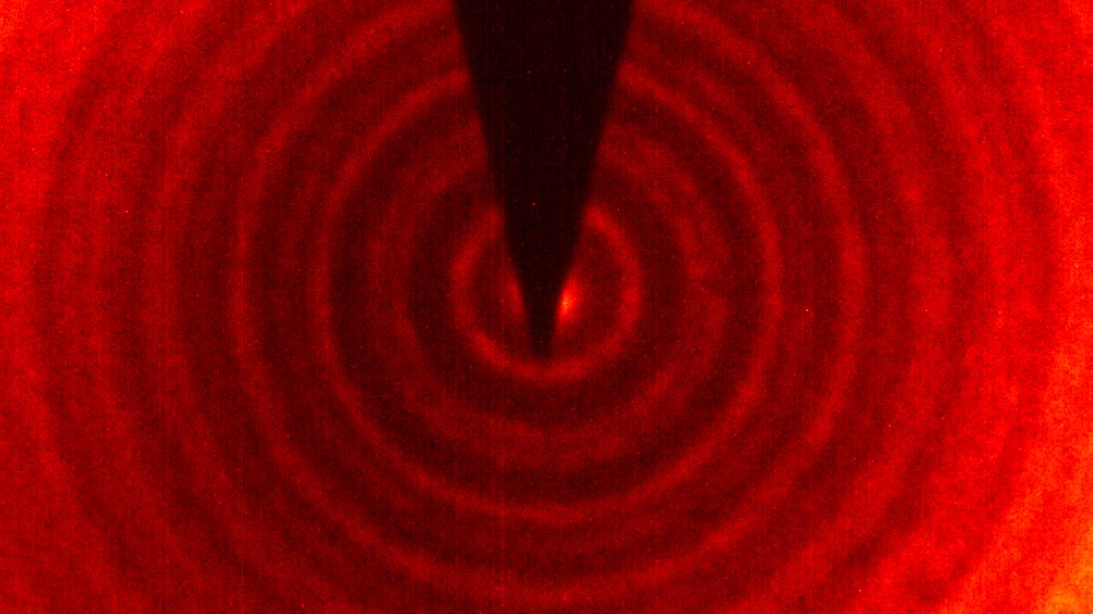
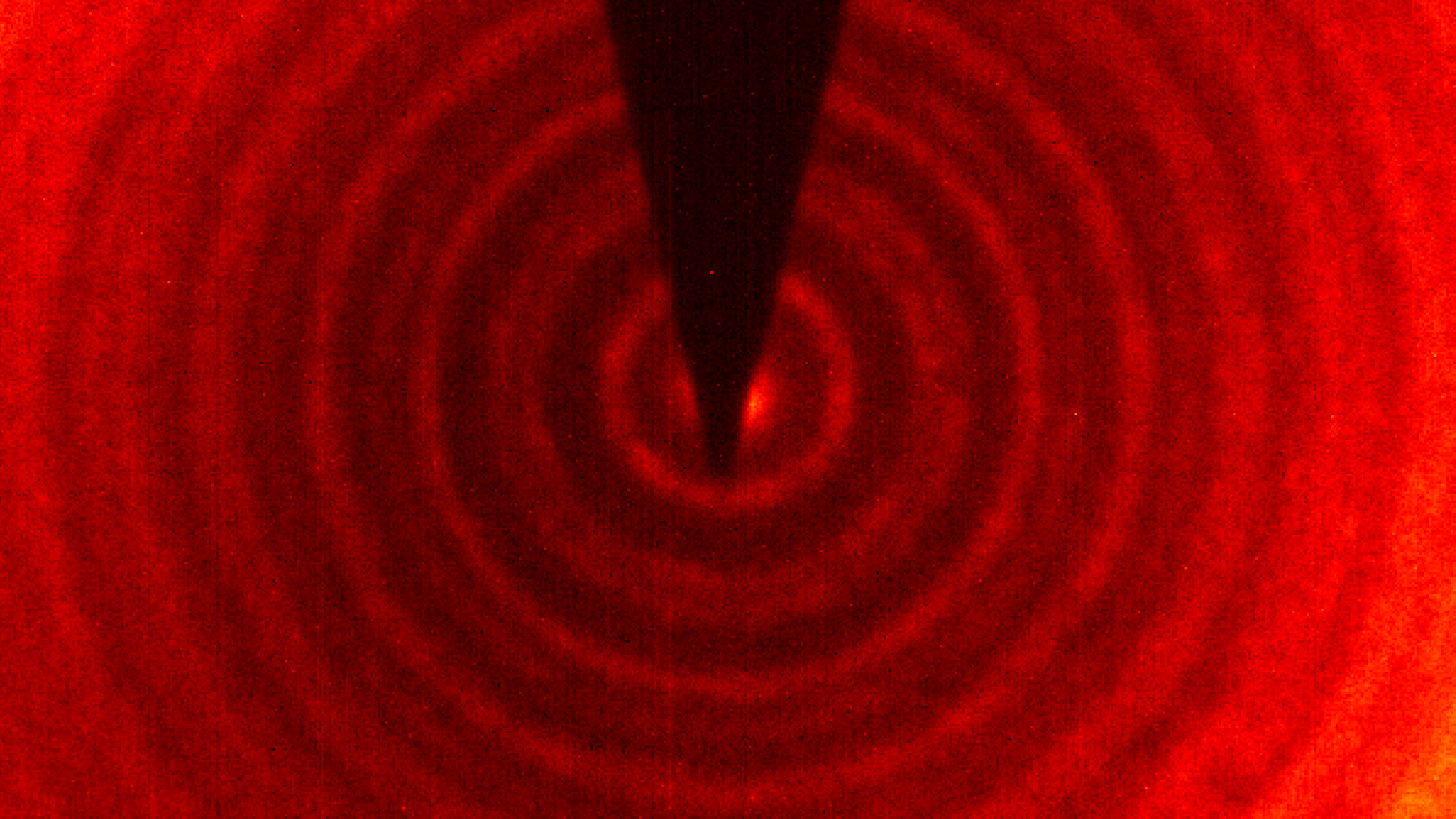
Researchers at DLR have for the first time diffracted a beam of helium atoms through an ultrathin graphene membrane. The atomic matter waves created a characteristic wave pattern behind the membrane.
Matter waves of atoms open up new avenues in materials analysis
In their laboratory, DLR researchers accelerated a beam of atoms to two million kilometres per hour towards a graphene sample. The matter waves of the atomic beam revealed information about the atomic structure of radiation-sensitive materials.
Schematic of the atomic beam diffraction experiment on solids
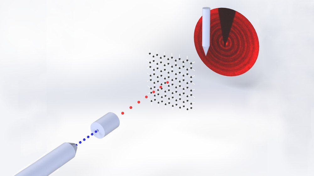
In a vacuum chamber, an ion source generates a beam of hydrogen or helium ions (blue dots). These are electrically neutralised and then, as atoms (red dots), strike a thin membrane of material – in this case graphene (the black grid). The membrane consists of a single layer of hexagonally-arranged carbon atoms. The matter waves of the atom beam diffracted by the graphene produce a characteristic interference pattern (red) on the detector screen. The pin in front of the detector blocks the direct atomic beam so only the deflected matter waves from the diffraction pattern remain visible.
DLR researchers have succeeded, for the first time, in diffracting matter waves of atoms through a solid; until now, this had only been possible with electrons and neutrons.
This opens up new avenues in materials research – enabling both the investigation of samples sensitive to radiation and the development of radiation-resistant materials.
The resulting diffraction pattern reveals information about the atomic structure of the material being examined.
Focus: Space, quantum technologies, materials research
Researchers at the German Aerospace Center (Deutsches Zentrum für Luft- und Raumfahrt; DLR) have succeeded for the first time in diffracting a beam of atoms through a solid. So far, this has only been possible with electrons or neutrons. The principle takes advantage of the fact that atoms can behave like waves – in a similar manner to water waves encountering an obstacle, matter waves form a characteristic pattern when they encounter an atomic lattice structure.
The potential applications of this are enormous: from materials research to nanotechnologies in industry and possibly even in medicine. The process may help to develop radiation-resistant materials, for example to improve the performance and longevity of electronics for spacecraft. The technology may also offer a gentler way to examine radiation-sensitive samples.
Materials research with matter waves
In materials research, biomedicine and chemistry, electron microscopy is an indispensable analytical tool. The wave-like behaviour of a beam of electrons – which, according to quantum theory, behave like both particles and waves – can be used to make individual atoms visible. This makes it possible, for example, to investigate the formation of crystals, detect foreign atoms or defects in atomic lattices and evaluate the quality of surfaces.
In transmission electron microscopy, a beam of electrons is passed through a thin sample material. This, however, exposes the sample to enormous amounts of radiation. "The radiation dose is locally so high that the method is not suitable for organic substances," explains Christian Brand from the DLR Institute of Quantum Technologies.
DLR is therefore developing new, non-destructive measurement methods for materials research. The technologies are based on matter waves of atoms. Atoms are larger than electrons but, in keeping with quantum theory, behave like both particles and waves – opening the door to non-destructive imaging analysis of atomic and molecular structures in solids and organic samples.
Through a solid at two million kilometres per hour!
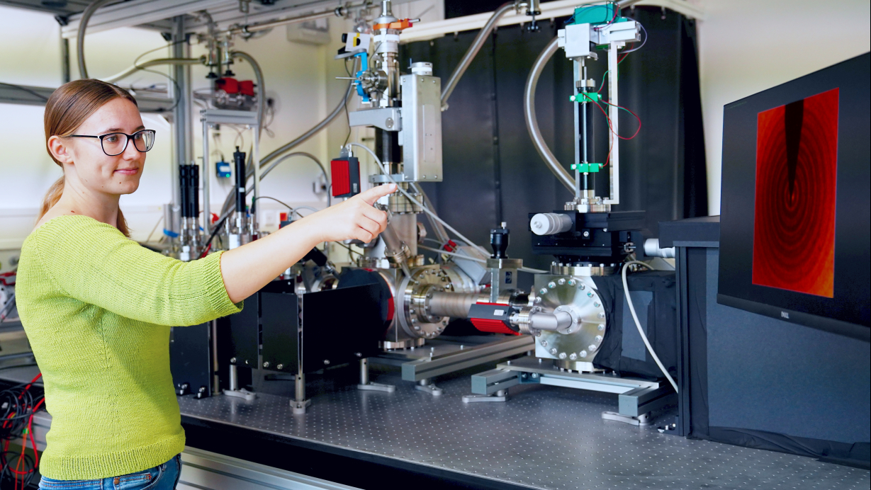
Researchers at the Institute of Quantum Technologies have achieved a world-first in diffracting a beam of atoms through a solid. In a vacuum chamber, they accelerated beams of hydrogen and helium atoms up to speeds of two million kilometres per hour, and passed them through an ultra-thin graphene membrane consisting of only a single layer of regularly-arranged carbon atoms.
When passed through the graphene membrane, the atomic beam revealed its quantum wave properties. As matter waves, individual atoms simultaneously interact with several carbon atoms in the sample. Like water waves around obstacles, they are deflected and then overlap behind the sample. This interference creates what is known as a diffraction pattern, which is visible on a detector screen. Based on the shape and size of the diffraction patterns, conclusions can be drawn about how the atoms are arranged in the material.
Matter waves of atoms open up new possibilities in materials research compared to electron or even neutron beams. The great advantage of atoms is that they are electrically neutral, so they interact with samples much more gently than electrons. With beams of atoms, it may be possible to determine the atomic or molecular structure of even radiation-sensitive materials, for example in organic chemistry and, potentially, in biology and medicine. Atomic beams are also easier to generate than neutron beams, which require large-scale facilities like a nuclear reactor.
Tailored velocity was the key
To record the diffraction pattern of matter waves, the atoms in the beam must not travel too slow or too fast. "The challenge was to keep the graphene membrane as clean as possible and to adjust the velocity of the beam of atoms so that we could clearly observe the diffraction effects," explains Carina Kanitz, who conducted the experiment. "Solids are usually too massive for atomic beams to penetrate – the atoms simply get stuck." However, the atoms must also not travel too quickly or the individual structures of the diffraction pattern will overlap and can no longer be distinguished.
"We naturally asked ourselves why the delicate quantum states of the atoms weren't destroyed passing through the sample – otherwise, there would have been no diffraction pattern like the ones we measured," adds Brand. The answer came from simulations from the Physics of Nanostructured Materials research group headed by Toma Susi at the University of Vienna. "The atoms travel so fast that they only have a millionth of a billionth of a second to interact with the sample. This is so short that the quantum states remain intact," explains Susi.
The hydrogen and helium atoms literally squeeze through the graphene membrane. "The faster the atoms travel through the membrane, the less time they have to interact with the carbon atoms in the membrane and the weaker the quantum physical interaction between the atom beam and the sample. The atom beam then behaves like a broad wave front, which penetrates the solid over a large area," adds Brand.
Solar wind in the lab for radiation-resistant electronics
DLR researchers now hope to test atomic diffraction on materials that are difficult to study using existing methods. Their focus is on organic materials such as polymer membranes for filter systems and materials used to make electronic components.
Graphene is just one of approximately 2000 known 'functional 2D materials' – at just one or two atoms thick, they often have special electrical properties. Atomically thin membranes have enormous potential as advanced materials for miniaturising electronic components. This makes them particularly interesting for space applications, ranging from miniature capacitors to quantum sensors for detecting electric and magnetic fields.
Atom-based matter wave technology can also help develop and test radiation-resistant materials. In space, particle radiation with energies similar to those used in the diffraction experiments is ubiquitous – for example in the solar wind, which can damage radiation-sensitive materials and electronic components on spacecraft. Radiation can break molecules apart and damage atomic lattices – imagine here tiny bullet holes. With the help of matter wave experiments, such challenging conditions can be recreated in the laboratory using atom, ion and electron beams. The goal is to gain a deeper understanding of how matter and particle beams interact, and how radiation damage can be avoided.
Background info: Matter waves and wave-particle duality
When light passes through a slit pattern, which is similar in scale to the size of its wavelength, a series of light and dark stripes appears – known as a diffraction pattern – on a screen behind the slits. In 1924, Louis de Broglie predicted the same phenomenon would appear with electron beams. In 1927, George Paget Thomson and, working separately, Clinton Davisson and Lester Germer, were able to experimentally demonstrate the diffraction of electron beams passing through crystals. This confirmation of de Broglie’s hypothesis earned him the 1929 Nobel Prize in Physics; Thomson and Davisson shared the 1937 award. The diffraction of matter waves laid the foundation for today's transmission electron microscopy.
Quantum objects, like electrons, have both wave- and particle-like properties. As waves, quantum objects are 'spread out' across space and can be in several places at once. Hence the probability distribution of finding a quantum object at any particular location behaves like a wave. However, when a measurement is made, quantum objects appear as particles – in only one place at a specific time. Quantum objects therefore possess both momentum and a wavelength – the apparent 'shift' from wave to particle upon measurement makes it impossible to know both their position and momentum at the same time, which is known as the 'uncertainty principle'.

