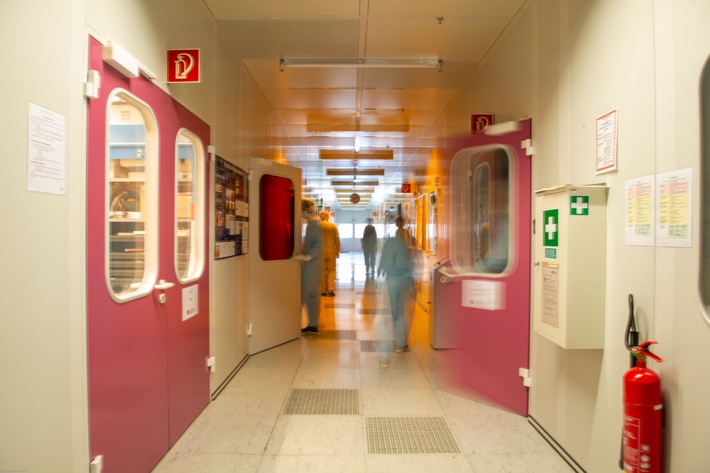
A view of the central laboratory corridor. More than 200 square metres of ISO 5 cleanroom space are available for diamond and microtechnology processes.
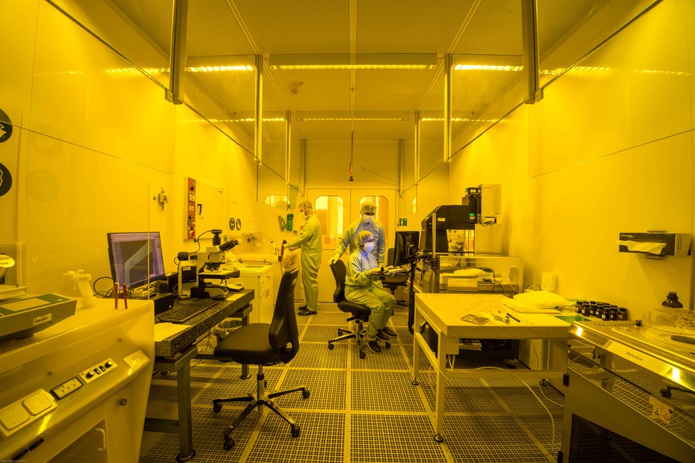
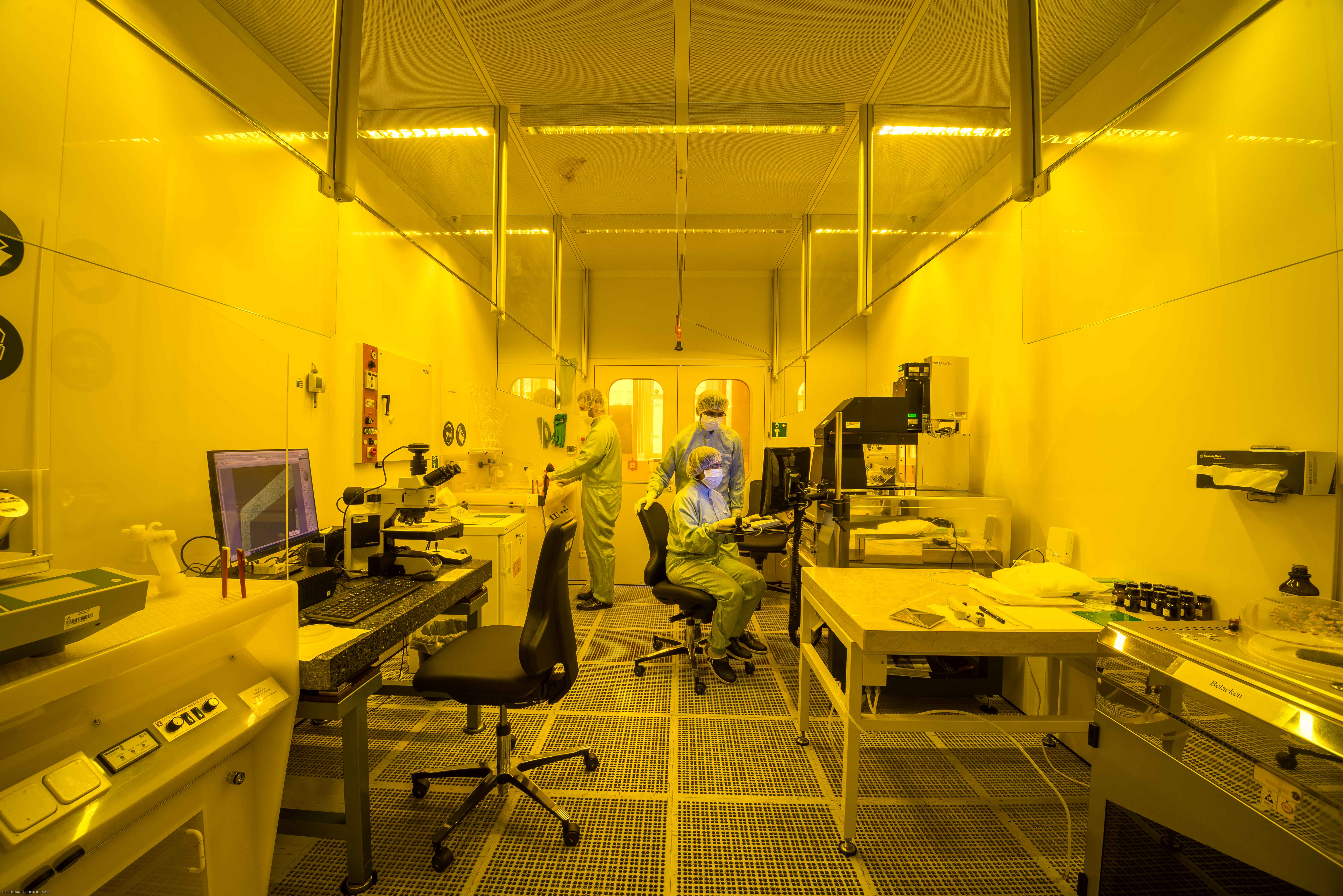
Nano- and microstructures are defined in the lithography laboratory. Yellow lighting prevents accidental exposure of UV‑sensitive photoresist layers that are processed in this area using photoresist coaters, UV mask alignment lights and developers.
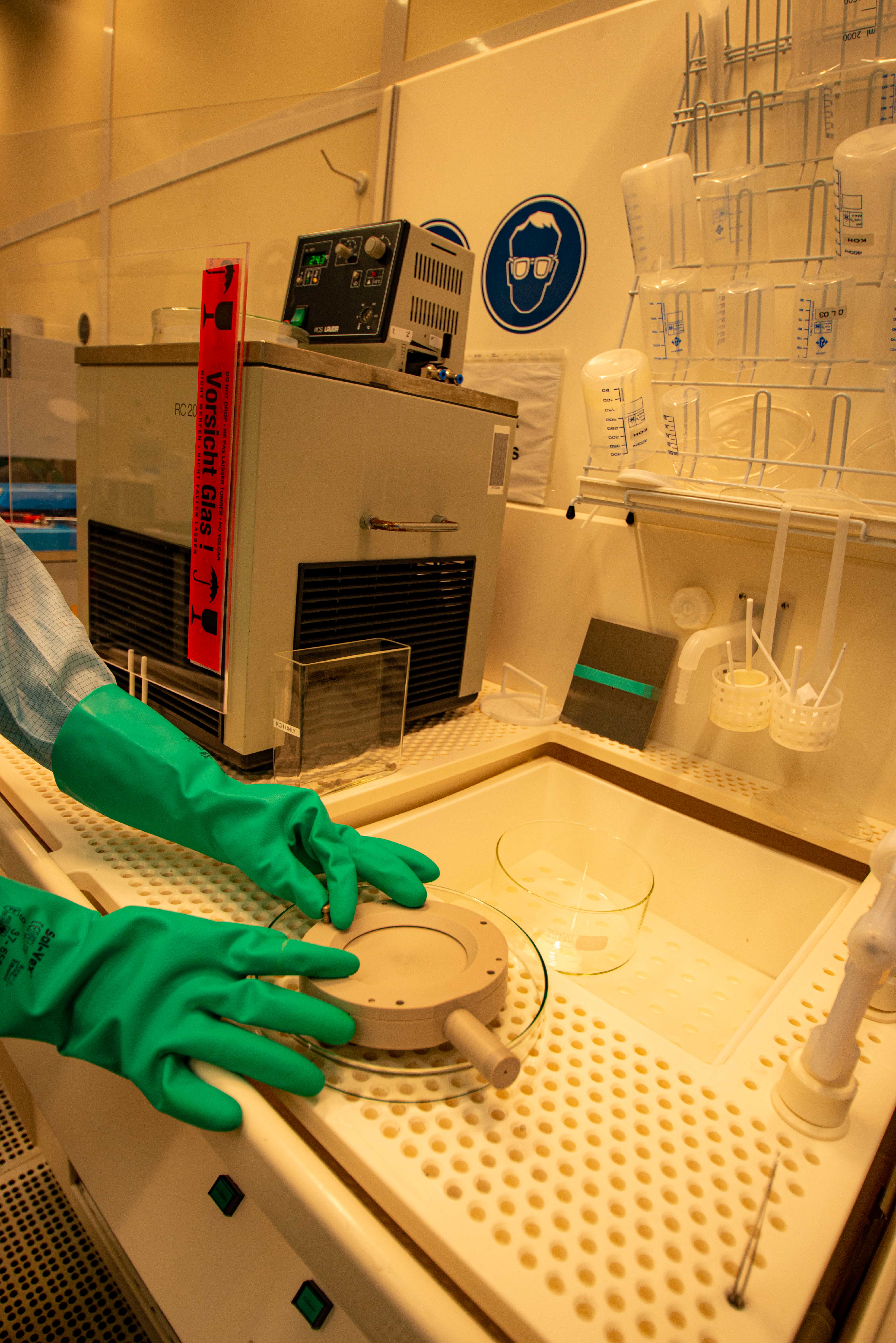
The chemical benches are equipped with a built-in extraction system in the worktop to guarantee laminar airflow and thereby minimise particle contamination. In these areas, wet-chemical etching processes are carried out at wafer level, for example with potassium hydroxide (KOH), for the anisotropic structuring of glass and silicon.
The DLR Institute of Quantum Technologies operates the Diamond Technology Cluster large-scale research facility. The technology cluster is geared towards the microproduction of quantum systems, particularly diamond-based materials. Competencies at the cluster range from micro- and nanofabrication all the way to assembly and interconnect technology, enabling the chip-level integration of quantum systems.
At this large-scale facility, wafers as well as silicon, glass and diamond substrates ranging from 1 to 150 millimetres can be structured using lithography. Thin-film deposition of metal films and dielectrics can also be performed. Substrates and films can be processed using a variety of dry and wet chemical etching techniques. Suitable optical microscopes and tactile measuring instruments are available for characterisation, capable of resolving structures in the nanometre and micrometre ranges. The infrastructure is complemented by dicing technology, various bonding techniques and wire and flip-chip bonders. When it comes to diamond processing, there are highly specialised systems for atomic layer deposition and etching using highly controlled plasma processes, as well as an implanter for creating defects. The entire laboratory is set up within an ISO 5 cleanroom environment and equipped with climate control for stable process conditions.
The entire process technology for manufacturing compact quantum systems is operated and continuously developed by the Integration of Micro- and Nanosystems department. In addition to complete technology components, individual processes or process chains can also be offered flexibly for projects and customer orders.
Equipment and processes
Characterisation technology
Prism coupler (refractive index)
White light interferometer
Surface profiler, profilometer
Confocal laser microscope
Optical microscope
Lithography
Semi-automatic coating system
Semi-automatic developer
UV lithography
Electron beam lithography
Implanter
Wet chemical process technology – solvents
Thin-film technology
PECVD SiO2, SiN
Electron beam evaporator
Thermal evaporator
Atomic layer deposition (ALD)
Etching technology
Wet chemical process technology for acids and bases (KOH, HF, HCI, etc.)
Microwave reactor for high-temperature acid and base processes
Plasma dry etching with fluorine‑based gases, including Bosch process (SF6, C4F8)
Plasma dry etching with chlorine gases
Plasma cleaning
Atomic layer etching (ALE)
Assembly and interconnect technology
Flip-chip bonder
Anodic bonding
Wafer bonder
Wire bonder (ball and wedge)
Ribbon wire bonder
Wafer saw
Chemical polishing
PEEK 3D printer
For further details about equipment and processes, please contact the institute directly.

